 There are numerous types of high density interconnect PCB to select from when doing prototyping, ranging from simple one-sided PCBs to extremely complex, multi-layer boards.
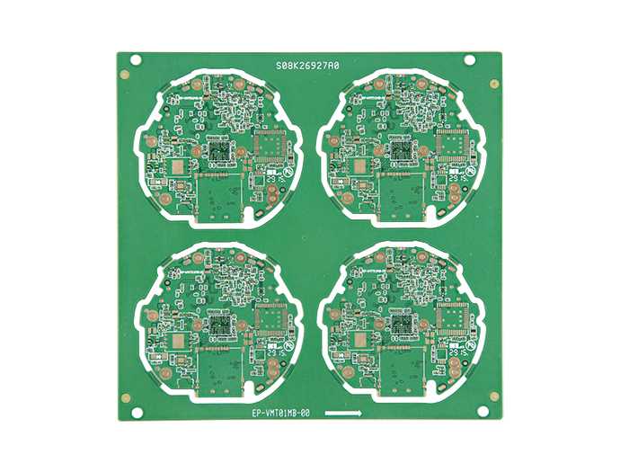
Typically, the most simple prototype hdi pcb are the ones that contain copper tracks, or interconnections between its components on only one of its surfaces. These boards are called as one-layer printed circuit boards, or single sided PCBs. However, in the manufacture of more complex circuit boards, there is a requirement for HDI PCBs. Known as High Density Interconnect, these printed circuit boards have a superior wiring density than traditional PCBs. Along with thinner spaces, smaller vias, and a higher connection pad density, and these boards brag a lot of dissimilar benefits to the typical prototype rigid flex pcb. One of the major features of HDI PCBs is that they not only utilize Vias to generate connections between layers, this type of circuits also utilizes Laser Drilled Microvias, which are smaller and more effectual in terms of space. Advantages of High Density Interconnect Technology Some advantages of these explicit printed circuit boards include: These PCBs are extremely compact - Considering that HDI PCBs have a superior wiring capacity, they are one of the finest alternatives for engineers looking for the smallest circuit board with the major output. HDI capacity makes it simpler to turn a 10 layered PCB into a four or else five coated one, which is huge for those searching for smaller boards without skimping on quality. Since most consumers favour small devices, this can be an enormous design advantage. The aptitude to place more components on one side - These HDI PCBs utilize blind as well as buried vias, along with Via-in-Pad technology, as procedures of placing components closer together, which consequences in faster signal transmission. Source: https://www.x-pcb.com
0 Comments
Leave a Reply. |
AuthorX-PCB Archives
March 2023
PCB |
 RSS Feed
